DC-DC Converter: Buck Converters
Published on February 16, 2025 | 👁️ 1291 Views
Introduction
DC-DC converters are essential components in modern-day electronics systems, enabling the transformation of voltage levels to meet the specific requirements of various devices.
In this article, we’ll be looking at the buck converter or step-down converter, a type of DC-DC converter which basically takes higher input voltage and converts it to a lower output voltage with high efficiency. We’ll cover the operation of buck converters, components involved, design consideration and some of the applications.
I hope you’re comfortable coz it’s gonna get deep.
The Operating Principle
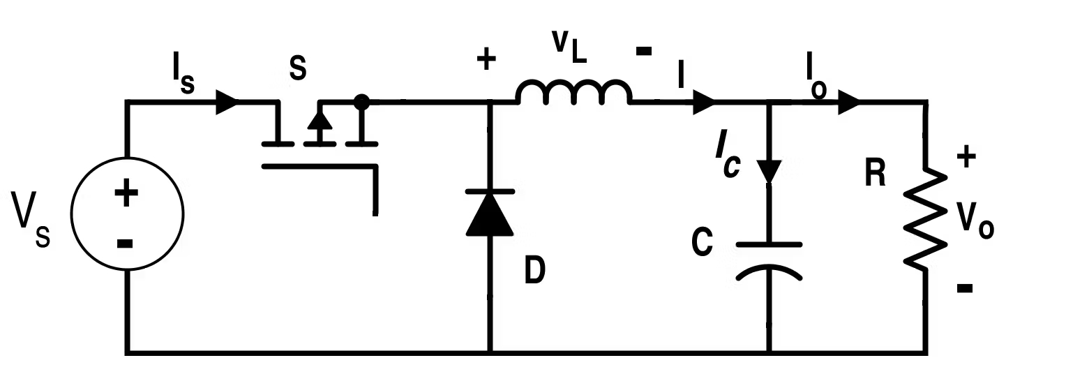
A buck converter efficiently reduces a higher DC input voltage to a lower DC output voltage. It achieves this through controlled switching elements (transistor), energy storage components (inductors), and filtering stages (Capacitors and diodes)

Basic Components
- Switching Element (Transistor): Typically a MOSFET, it controls the connection between the input voltage and the inductor.
- Diode: Provides a path for inductor current when the switching element is off. In synchronous buck converters, a second MOSFET replaces the diode to improve efficiency.
- Inductor: Stores energy when the switch is on and releases it when the switch is off, smoothing the current to the load.
- Output Capacitor: Filters the output voltage, reducing ripple and providing a stable DC output.
- Control Circuitry: Generates the pulse-width modulation (PWM) signal to control the switching element, regulating the output voltage.
The buck converter operates in two distinct phases based on the switching state of \(S\).
Mode 1: Switch \(S\) is ON (Conducting State)
- The MOSFET (or switch) is closed, creating a direct connection between \(V_s\) and the inductor \(L\)
- The inductor stores energy as current flows through it.
- The diode \(D\) is reverse biased and does not conduct.
- The capacitor\(C\) supplies the load while also charging up for later use.
Inductor Voltage & Current
Using Faraday’s Law, the voltage across the inductor is:
$$ V_L = V_s - V_o $$
The inductor current increases as:
$$ \frac{dI_L}{dt} = \frac{V_s - V_o}{L} $$
This continues for the on-time \(t_{\text{ON}} \) of the switch.
Mode 2: Switch \(S\) is OFF (Non-Conducting State)
- The switch \(S\) opens, disconnecting the inductor from the supply.
- The inductor maintains current flow by releasing stored energy.
- The diode \(D\) turns ON (forward-biased), providing a path for inductor current.
- The capacitor helps regulate the voltage by supplying charge to the load.
Inductor Current During OFF State
Now, the inductor voltage reverses:
$$ V_L = -V_o $$
And the current decreases:
$$ \frac{dI_L}{dt} = \frac{-V_o}{L} $$
This continues during the off-time \(t_{\text{OFF}} \) of the switch.
Mathematical Expression for Output Voltage
The average output voltage is determined by the duty cycle \(D\), defined as:
$$ D = \frac{t_{\text{ON}}}{T} $$
where \(T\) is the switching period.
Since the inductor’s steady-state voltage over a full cycle must be zero:
$$ V_o = D \cdot V_s $$
This means the output voltage is always lower than the input voltage, making it a step-down (buck) converter.
Current & Voltage Waveforms
-
Inductor Current (\(I_L \)):
- Rises when \(S\) is ON.
- Falls when \(S\) is OFF.
- Remains continuous in Continuous Conduction Mode (CCM).
- Output Voltage (\( V_o \)):
- Remains relatively constant due to the capacitor’s filtering action.
- A small ripple may be present.

Design Considerations
Designing an efficient and reliable buck converter involves careful selection and sizing of components based on the desired performance criteria.
Inductor Selection
The inductor value (\(L\)) influences the ripple current and the mode of operation. It is chosen based on the acceptable ripple current $$ \Delta I_L $$ and is calculated as:
$$ L = \frac{(V_{in} - V_{out}) \times D}{f_s \times \Delta I_L} $$
Where:
- \( f_s\) is the switching frequency
Capacitor Selection
The output capacitor is responsible for smoothing the output voltage and reducing the voltage ripple. The required capacitance can be estimated using:
$$ C_{out} = \frac{I_{load} \cdot D}{f_s \cdot \Delta V_{out}} $$
Where:
- \(I_{\text{load}}\) is the load current,
- \(D\) is the duty cycle
- \(f_s\) is the switching frequency
- \(\Delta V_{\text{out}}\) is the allowable output voltage ripple
To further reduce ripple, a low Equivalent Series Resistance (ESR) capacitor is preferred.
Diode Selection
In a non-synchronous buck converter, the freewheeling diode should have:
- A fast recovery time (Schottky diodes are preferred).
- Duration it takes for a diode to switch from conducting (forward-biased) to non-conducting (reverse-biased) when the applied voltage changes
- A current rating at least equal to the inductor peak current.
- A reverse voltage rating greater than the input voltage.
For synchronous buck converters, the diode is replaced with a MOSFET for improved efficiency.
MOSFET Selection
The high-side MOSFET is the main switching component. The key parameters to consider:
- Drain-Source Voltage \( V_{DS} \geq V_{in}\)
- Current Rating \( I_D \geq \) Peak Inductor Current
- Low Rds(ON) for minimizing conduction losses
- Gate Charge \( Q_g :\) Lower values reduce switching losses.
In synchronous buck converters, a low-side MOSFET is used in place of the diode.
Switching Frequency Selection
The switching frequency \(f_s\) significantly affects efficiency. A higher switching frequency reduces the inductor size but increases switching losses.
Typical values:
- Low-power applications: \( f_s = 100 \text{ kHz} - 500 \text{ kHz} \)
- High-frequency designs: \( f_s = 1 \text{ MHz} - 3 \text{ MHz}\)
An optimal tradeoff between inductor size and efficiency is required.
$$ P_{\text{switching}} = V_{in} \cdot I_{\text{load}} \cdot f_s \cdot Q_g $$
Efficiency Analysis
The efficiency of a buck converter is determined by the ratio of output power to input power:
$$ \eta = \frac{P_{\text{out}}}{P_{\text{in}}} \times 100\% $$
Where:
- \( P_{\text{out}} = V_{\text{out}} \cdot I_{\text{out}}\)
- \(P_{\text{in}} = V_{\text{in}} \cdot I_{\text{in}} \)
Losses occur due to:
- Conduction Losses (\( P_{\text{cond}} \)):
$$ P_{\text{cond}} = I_{\text{load}}^2 \cdot (R_{\text{DS(ON)}} + R_{\text{inductor}}) $$
- Switching Losses (\( P_{\text{switching}} \)):
$$ P_{\text{switching}} = \frac{1}{2} V_{\text{in}} I_{\text{load}} f_s (t_r + t_f) $$
where \(t_r \) and \( t_f \) are the rise and fall times of the MOSFET.
- Diode Conduction Losses (if using a diode):
$$ P_{\text{diode}} = V_f \cdot I_{\text{load}} \cdot (1 - D) $$
where \(V_f\) is the forward voltage drop of the diode
Control Techniques
Modern buck converters use feedback control to regulate output voltage. There are two primary methods:
- Voltage Mode Control (VMC):
- Uses a single feedback loop.
- Simple to implement but suffers from poor transient response.
- Requires compensation circuits for stability.
- Current Mode Control (CMC):
- Adds inductor current sensing, making it faster and more stable.
- Provides automatic current limiting.
The control law is often implemented using a Pulse Width Modulation (PWM) signal:
$$ D = \frac{V_{\text{out}}}{V_{\text{in}}} $$
where \(D\) is the duty cycle
Transient Response & Stability
A load transient occurs when the current demand from the load changes suddenly. This can cause an undesirable deviation in output voltage, leading to potential issues in sensitive electronic circuits.
The goal of transient response optimization is to minimize voltage deviations and ensure that the output voltage returns to its nominal value as quickly as possible.
Key Factors Affecting Transient Response
1. Inductor Value \(L\)
The choice of the inductor value plays a critical role in transient response.
Larger Inductor (\( L \uparrow \) ):
- Slower transient response (longer time to adjust).
- Lower output voltage ripple.
- Less stress on the output capacitor.
Smaller Inductor (\( L \downarrow\)):
- Faster transient response (output voltage recovers quickly).
- Higher ripple current (may require better capacitors or advanced control techniques).
Inductor Current During Transient Events
The inductor current response is governed by:
$$ \frac{dI_L}{dt} = \frac{V_{\text{in}} - V_{\text{out}}}{L} $$
- A lower inductor value \( L \downarrow\) increases \( \frac{dI_L}{dt}\), allowing the current to adjust more quickly.
- However, too small an inductor leads to excessive ripple current and may force operation into discontinuous conduction mode (DCM), reducing efficiency
2. Output Capacitor Value \( C_{\text{out}}\)
The output capacitor filters out voltage deviations and stabilizes the output during transient events.
Role of the Output Capacitor
-
During a load step-up event, the capacitor provides extra current before the inductor can respond.
- During a load step-down event, the capacitor absorbs excess energy to prevent voltage overshoot.
Capacitor Sizing
The required capacitance is estimated using:
$$ C_{\text{out}} \geq \frac{I_{\text{load-step}}}{f_s \cdot \Delta V_{\text{out}}} $$
where:
- \(I_{\text{load-step}}\) is the change in load current
- \(f_s\) is the switching frequency
- \(\Delta V_{\text{out}}\) is the acceptable voltage deviation
Larger Capacitor (\( C_{\text{out}} \uparrow\)):
- Reduces voltage deviation.
- Improves transient response.
- Increases size and cost (ceramic capacitors preferred for fast response).
Smaller Capacitor (\(C_{\text{out}} \downarrow\)):
- Faster response in control loop.
- Less effective filtering (may require additional filtering components).
Ceramic capacitors (low ESR) are preferred over electrolytic capacitors due to their fast response time.
Commonly Used Buck Converters & Their Applications
There are several integrated buck converter ICs that are widely used in the industry due to their high efficiency, ease of use, and reliability. Below are some of the most common ones:
1. LM2596 (Texas Instruments)
Features:
- Input Voltage: 4V - 40V
- Output Voltage: Fixed 3.3V, 5V, 12V, or adjustable
- Max Output Current: 3A
- Switching Frequency: 150 kHz
- Efficiency: ~80-90%
Applications:
- Arduino & Raspberry Pi Power Supplies
- Battery-Powered Embedded Systems
- General-Purpose DC-DC Conversion in DIY Electronics
This is one of the most commonly used buck converters in hobbyist projects and low-power embedded systems due to its simplicity and reliability.
2. MP2315 (Monolithic Power Systems)
Features:
- Input Voltage: 4.5V - 24V
- Output Voltage: Adjustable (0.8V to 22V)
- Max Output Current: 3A
- High Switching Frequency: 500 kHz
- Built-in Overcurrent & Thermal Protection
Applications:
- Laptop & Computer Motherboards
- FPGA & Microcontroller Power Rails
- High-Efficiency DC-DC Conversion in Industrial Applications
This buck converter is known for its high efficiency and small size, making it perfect for embedded applications.
Advanced Buck Converter Variants
- Synchronous Buck Converter:
- Replaces the diode with a MOSFET to reduce losses.
- Higher efficiency at low output voltages.
- Multiphase Buck Converter:
- Uses multiple inductors & MOSFETs.
- Improves efficiency for high-current loads (e.g., CPU power supplies).
- Soft-Switching Buck Converters:
- Techniques like ZVS (Zero Voltage Switching) and ZCS (Zero Current Switching) reduce switching losses.
Conclusion
The DC-DC buck converter is one of the most widely used power conversion circuits, offering high efficiency, precise voltage regulation, and compact design. Understanding its principles, component selection, efficiency factors, and control techniques is essential for designing reliable power electronics systems.
Comments
-
Carlo - 11 months ago
Can you do one for a buck-boost please
-
Anonymous - 11 months ago
great work dude!

